DDS直接数字合成2 - 任意信号
为了生成任意信号,DDS 依赖于两个主要技巧。
LUT
第一个 DDS 技巧是 LUT(查找表)。 LUT 是一个表格,用于保存我们想要生成的模拟信号的形状。
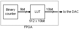
在FPGA中,LUT是作为blockram实现的。 在上图中,我们使用了 512x10 位 LUT,它通常适合一个或两个物理 FPGA 模块。
正弦波
最常产生的信号形状是正弦波。 它很特别,因为它有两个对称性,可以很容易地利用它们来使 LUT 看起来更大。
在正弦波中,第一个对称性是sin(α)=sin(π-α)。
假设我们的 “my_DDS_LUT” blockram 是这样实例化的
wire [9:0] LUT_output;

blockram512x10bit_2clklatency my_DDS_LUT(.rdclock(clk), .rdaddress(cnt[8:0]), .q(LUT_output));
我们只需要在半个周期后以相反的方向访问 LUT 即可利用第一个对称性。
blockram512x10bit_2clklatency my_DDS_LUT(.rdclock(clk), .rdaddress(cnt[9] ? ~cnt[8:0] : cnt[8:0]), .q(LUT_output));
因此,现在我们只将一半的波存储在模块中,但其内容在输出信号的每个周期中使用两次。 从某种意义上说,LUT 显示为 1024x10 位(使用第二种对称性,我们得到 2048x10 位)。
请注意,我们使用一个块“blockram512x10bit_2clklatency”,它提供具有两个时钟延迟的数据(因为一个时钟延迟块框速度较慢)。 如何做到这一点取决于FPGA供应商(Altera将使用LPM,而Xilinx将使用原语)。
让我们将 LUT 重写为一个单独的模块,利用两个正弦对称性。
// sine lookup value module using two symmetries
// appears like a 2048x10bit LUT even if it uses a 512x10bit internally
// 3 clock latencymodule sine_lookup(input clk, input [10:0] addr, output reg [16:0] value);
wire [15:0] sine_1sym;  // sine with 1 symmetry
blockram512x16bit_2clklatency my_quarter_sine_LUT(     // the LUT contains only one quarter of the sine wave
    .rdclock(clk),
    .rdaddress(addr[9] ? ~addr[8:0] : addr[8:0]),   // first symmetry
    .q(sine_1sym)
);

// now for the second symmetry, we need to use addr[10]
// but since our blockram has 2 clock latencies on reads
// we need a two-clock delayed version of addr[10]
reg addr10_delay1;
always @(posedge clk) addr10_delay1 <= addr[10];
reg addr10_delay2; always @(posedge clk) addr10_delay2 <= addr10_delay1;
wire [15:0] sine_2sym = addr10_delay2 ? {1'b0,-sine_1sym} : {1'b1,sine_1sym};  // second symmetry

// add a third latency to the module output for best performance
always @(posedge clk) value <= sine_2sym;
endmodule
请注意,sine_lookup模块总共有 3 个时钟延迟(两个来自模块,一个来自末尾的注册输出)。
时钟延迟的好处是可以流水线操作,并从FPGA中获得最大可能的性能。 不要忘记,这需要运行至少 100MHz。
此外,我们还将 blockram 的输出宽度从 10 位增加到 16 位(如果在我们的特定 FPGA 模块中未使用,则 6 位会丢失,因此我们不妨实现它们)。 我们将在第 4 部分中充分利用多余的部分。
为了有效地使用我们新制作的“sine_lookup模块”,我们可以简单地编写
reg [10:0] cnt;
always @(posedge clk) cnt <= cnt + 11'h1;
wire [16:0] sine_lookup_output;
sine_lookup my_sine(.clk(clk), .addr(cnt), .value(sine_lookup_output));
wire [9:0] DAC_data = sine_lookup_output[16:7];   // for now, we drop the LSBs to feed our DAC
                                                  // (since it takes only 10 bits)
我们从DAC得到一个很好的正弦波。
上一篇:DDS直接数字合成1 - 简介

加入微信
获取电子行业最新资讯
搜索微信公众号:EEPW
或用微信扫描左侧二维码