T W AC 0100 | Internal 1V reference always powered; write ADC control word with 表5. 外部基准命令 DEMO1234 Command | Action | SPI data in | T W AC 0300 | External reference must be provided;2.3) 测量外部电压输入AUX1和AUX2表6. ADC测量命令序列 DEMO1234 Command | Action (Triggered by A/D3210 Bits) | SPI data in | T M8 | Measure AUX1 with 12-bit resolution and 3.5µs conversion rate | 0x0040 0x2301 0x8008 0x0000 |
0x8005 0x0000 | T W AC 1b01 | Trigger ADC scan of BAT1;0x8006 0x0000 |
0x8009 0x0000 |
T W AC 2b01 | Trigger ADC scan of TEMP1;0x8009 0x0000 2.8) 将TEMP1转换结果译为物理值下面的C/C++伪代码片断总结了DEMO1234程序是怎样解释TEMP1转换结果的。 /* ADC control resolution value selects num_codes 4096 (12-bit), 1024 (10-bit), or 256 (8-bit) */int num_codes = 4096; /* ADC_control_RES11: 12-bit resolution *//* Voltage that corresponds to the full-scale ADC code; may be internal 1V or 2.5V ref, or ext ref. */double ADC_fullscale_voltage = 2.5; /* ADC_control_RFV=1: VREF=2.5V. RFV=0: VREF=1.0V. *//* TEMP1_code is the 16-bit result read by SPI command 0x8009 */double TEMP1_Voltage = (TEMP1_code * ADC_fullscale_voltage) / num_codes;/* Calibration values */const double Temp1V_Room = 0.590; // temp1 voltage at room temperature 25Cconst double Temp1K_Room = 298.15; // Room temperature Kelvins (298.15K=25C)const double Temp1V_Per_K = -0.002; // TempCo -2mV per degree C/* Convert to absolute temperature */double Kelvin = (TEMP1_Voltage - Temp1V_Room) / Temp1V_Per_K + Temp1K_Room;/* Optional conversion to commonly used temperature units */double Centigrade = Kelvin - 273.15;double Fahrenheit = (Centigrade * 9.0 / 5.0) + 32; 2.9) 将TEMP1和TEMP2转换结果译为物理值下面的C/C++伪代码片断总结了DEMO1234程序是怎样解释TEMP1和TEMP2转换结果的。TEMP2只在和TEMP1对比时才有意义。 /* ADC control resolution value selects num_codes 4096 (12-bit), 1024 (10-bit), or 256 (8-bit) */int num_codes = 4096; /* ADC_control_RES11: 12-bit resolution *//* Voltage that corresponds to the full-scale ADC code; may be internal 1V or 2.5V ref, or ext ref. */double ADC_fullscale_voltage = 2.5; /* ADC_control_RFV=1: VREF=2.5V. RFV=0: VREF=1.0V. *//* TEMP1_code is the 16-bit result read by SPI command 0x8009 */double TEMP1_Voltage = (TEMP1_code * ADC_fullscale_voltage) / num_codes;/* TEMP2_code is the 16-bit result read by SPI command 0x800a */double TEMP2_Voltage = (TEMP2_code * ADC_fullscale_voltage) / num_codes;/* Calibration values */const double K_Per_Temp21_Delta_V = 2680.0; // nominal 2680 5/27/2002/* Convert to absolute temperature */double Kelvin = (TEMP2_Voltage - TEMP1_Voltage) * K_Per_Temp21_Delta_V;/* Optional conversion to commonly used temperature units */double Centigrade = Kelvin - 273.15;double Fahrenheit = (Centigrade * 9.0 / 5.0) + 32; 2.10) 测量外部电压输入AUX1、AUX2、BAT1、BAT2和温度表9. ADC测量命令序列 DEMO1234 Command | Action (Triggered by A/D3210 Bits) | SPI data in | T MB | Measure BAT1/4, BAT2/4, AUX1, AUX2, TEMP1, TEMP2 with 12-bit resolution and 3.5µs conversion rate | 0x0040 0x2f01 0x8006 0x0000 0x8008 0x0000 0x800a 0x0000 | T W AC 2f01 | Trigger ADC scan of BAT1-2, AUX1-2, TEMP1-2;3) 触摸屏实例下面的例子解释了怎样使用DEMO1234.EXE程序来获得触摸屏数据。3.1) 低成本商用触摸屏在互联网上搜索"PDA Digitizer/Glasstop",寻找合适的替代触摸屏。高清触摸屏玻璃的价格范围在50美元至10美元之间,价格取决于型号以及玻璃是否全部贴在显示屏上。3.2) 连接触摸屏和评估板MAX1234评估板提供突出插头H5/H6来连接10mm柔性电缆或者长度更短的电缆。H6连接器的间距是0.5mm,比实际触摸屏柔性电缆间距更精细。把柔性电缆插入H6,上锁,选择位于四条柔性电缆中每一电缆中心位置的H5引脚。跳接器连接H5和标有U1的X+、Y+、X-以及Y-测试点。3.3) 检验触摸屏的连接第一次连接触摸屏时,通过下面的步骤来验证X和Y连接是否正确。可以有几个触摸屏交叉连接,但大部分不会正常工作。在这些例子中,我们假设X- = left,X+ = right,Y- = top,Y+ = bottom。表10. 触摸屏物理连接验证命令序列 DEMO1234 Command | Action | SPI data in | Verification | | Connect DVM to X+/GND | | | T MD | No measurement; drive Y+,Y- | 0x0040 0x3701 | | | Touch top left | | X+ = approx. Y- | | Touch top right | | X+ = approx. Y- | | Touch bottom left | | X+ = approx. Y+ | | Touch bottom right | | X+ = approx. Y+ | | Connect DVM to Y+/GND | | | T ME | No measurement; drive X+,X- | 0x0040 0x3b01 | | | Touch top left | | Y+ = approx. X- | | Touch top right | | Y+ = approx. X+ | | Touch bottom left | | Y+ = approx. X- | | Touch bottom right | | Y+ = approx. X+ |
3.4) 检测触摸屏的操作:根据需要扫描在配置MAX1234检测触摸屏操作,根据需要数字化接触屏的位置时,写入寄存器0x40 (ADC控制),其PENSTS=0,ADSTS=0 (请参考MAX1233/MAX1234数据资料的表6)。读取寄存器0x00 (X轴)后,检测到后续的触摸屏操作时,/PENIRQ信号锁存至低电平,在写入ADC控制寄存器测量X、Y轴之前,保持低电平。 表12. 触摸屏检测命令序列:根据需要扫描 DEMO1234 Command | Action | SPI data in | Verification | T W AC 0b01 | Demand scan | 0x0040 0x0b01 | | T R AX | Read conversion result register X | 0x8000 0x0000 | | P R 6 | Read PENIRQ-bar pin status | | PENIRQ = 1 | | Touch the touch screen | | | P R 6 | Read PENIRQ-bar pin status | | PENIRQ = 0 | T M2 | Measure X,Y,Z1,Z2 | 0x0040 0x0b01 0x8001 0x0000 0x8003 0x0000 | | P R 6 | Read PENIRQ-bar pin status | | PENIRQ = 1 | | Touch and hold the touch screen | | | P R 6 | Read PENIRQ-bar pin status | | PENIRQ = 0 | T M2 | Measure X,Y,Z1,Z2 | 0x0040 0x0b01 0x8001 0x0000 0x8003 0x0000 | | P R 6 | Read PENIRQ-bar pin status | | PENIRQ = 0 | T M2 | Measure X,Y,Z1,Z2 | 0x0040 0x0b01 0x8001 0x0000 0x8003 0x0000 | | P R 6 | Read PENIRQ-bar pin status | | PENIRQ = 0 | | Release the touch screen | | | P R 6 | Read PENIRQ-bar pin status | | PENIRQ = 0 | T M2 | Measure X,Y,Z1,Z2 | 0x0040 0x0b01 0x8001 0x0000 0x8003 0x0000 | | P R 6 | Read PENIRQ-bar pin status | | PENIRQ = 1 |
表13. 触摸屏检测命令序列:自动扫描 DEMO1234 Command | Action | SPI data in | Verification | | Optional: connect oscilloscope to PENIRQ-bar | | | I C 1 3 | Configure PENIRQ-bar pulse accumulator: falling-edge trigger | | | I 0 1 | Reset the pulse accumulator | | | I R 1 | Read the number of times PENIRQ-bar has pulsed low | | count = 0 | T W AC 8bff | Wait for touch, then scan X,Y,Z1,Z2 | 0x0040 0x8bff | | | Touch the touch screen | | PENIRQ pulse | I R 1 | Read the number of times PENIRQ-bar has pulsed low | | count has increased | T R P | Read X,Y,Z1,Z2 conversion results | 0x8000 0x0000 0x8002 0x0000 0x8001 0x0000 0x8003 0x0000 | | | Touch the touch screen | | PENIRQ pulse | I R 1 | Read the number of times PENIRQ-bar has pulsed low | | count has increased | T R P | Read X,Y,Z1,Z2 conversion results | 0x8000 0x0000 0x8002 0x0000 4) 键盘和通用输入/输出引脚下面的例子介绍了怎样使用DEMO1234.EXE程序来扫描键盘,怎样使用GPIO键盘扫描引脚。4.1) 配置键盘和GPIO引脚GPIO控制寄存器将每个C1–C4和R1–R4引脚分别配置为输入、输出或者是键盘的一部分(请参考MAX1233/MAX1234数据资料的表26和表27)。此外,写入GPIO上拉禁止寄存器,将输出引脚配置为开漏输出。表14. 键盘和GPIO配置实例 DEMO1234 Command | Action | SPI data in | T W GC FFFF | Keypad: none;GPIO inputs: none | 0x004f 0xffff | T W GC FF00 | Keypad: none;GPIO outputs: none;GPIO outputs: C4,C3;4.2) 读写GPIO引脚GPIO数据寄存器读取GPIO输入引脚,写入GPIO输出引脚。注意:在这些例子中,C3、C4和R4是引脚名称,而不是元件名称。表15. GPIO实例 DEMO1234 Command | Action | SPI data in | Verification | T W GC C8C0 | Keypad:4.3) 检测按键:自动扫描可以配置键盘控制寄存器在探测到有按键按下时,自动扫描键盘。表16. 按键命令序列:自动扫描 DEMO1234 Command | Action | SPI data in | Verification | | Optional: connect oscilloscope to KEYIRQ-bar | | | I C 0 3 | Configure KEYIRQ-bar pulse accumulator: falling-edge trigger | | | I 0 0 | Reset the pulse accumulator | | | I R 0 | Read the number of times KEYIRQ-bar has pulsed low | | count = 0 | T W GC 0000 | Keypad:4.4) 从键盘中屏蔽单个按键使用键盘屏蔽寄存器和键盘2结果寄存器来屏蔽每个按键。屏蔽掉的按键被扫描至KPD寄存器,但是不在键盘2结果寄存器中报告。表17. 按键命令序列:屏蔽单个按键 DEMO1234 Command | Action | SPI data in | Verification | T W GC 0000 | Keypad:4.5) 从键盘中屏蔽一列使用键盘列寄存器来屏蔽所有列。不扫描屏蔽列,因此,KPD寄存器不会探测这些列中的按键。表18. 按键命令序列:屏蔽键盘的一列 DEMO1234 Command | Action | SPI data in | Verification | T W GC 0000 | Keypad:5) 电源管理表19. 关断命令 DEMO1234 Command | Action | SPI data in | Verification | T W AC C000 | Power off ADC | 0x0040 0xc000 | — | T W AC 0300 | Power off internal reference | 0x0040 0x0300 | REF = not driven | T W DC 8000 | Disable DAC | 0x0042 0x8000 | DACOUT = 0.0V | T W KC C000 | Power off keypad | 0x0041 0xc000 | — |
CmodComm测试程序主菜单—在连接前对C (连接)命令的响应Board connected.Got board banner: Maxim MINIQUSB V01.05.41 主菜单—连接后有效R) CmodBoardReset测试菜单命令—连接后有效6.1) 寄存器读/写命令表20. 读取寄存器助记符 DEMO1234 Command | Mnemonic | SPI data in | T R A1 | Test Read AUX1 register | 0x8007 0x0000 | T R A2 | Test Read AUX2 register | 0x8008 0x0000 | T R AC | Test Read ADC_control register | 0x8040 0x0000 | T R AX | Test Read X register | 0x8000 0x0000 | T R AY | Test Read Y register | 0x8001 0x0000 | T R AZ1 | Test Read Z1 register | 0x8002 0x0000 | T R AZ2 | Test Read Z2 register | 0x8003 0x0000 | T R B1 | Test Read BAT1 register | 0x8005 0x0000 | T R B2 | Test Read BAT2 register | 0x8006 0x0000 | T R DC | Test Read DAC_control register | 0x8042 0x0000 | T R DD | Test Read DAC_data register | 0x800b 0x0000 | T R GC | Test Read GPIO_control register | 0x804f 0x0000 | T R GD | Test Read GPIO_data register | 0x800f 0x0000 | T R GP | Test Read GPIO_pullup register | 0x804e 0x0000 | T R K1 | Test Read KPDATA1 register | 0x8010 0x0000 | T R K2 | Test Read KPDATA2 register | 0x8011 0x0000 | T R KB | Test Read KPD register | 0x8004 0x0000 | T R KC | Test Read KEY_control register | 0x8041 0x0000 | T R KK | Test Read KPCOLMASK register | 0x8051 0x0000 | T R KM | Test Read KPKEYMASK register | 0x8050 0x0000 | T R T1 | Test Read TEMP1 register | 0x8009 0x0000 | T R T2 | Test Read TEMP2 register | 0x800a 0x0000 |
表22. 触摸屏测量命令序列 DEMO1234 Command | Action (Triggered by A/D3210 Bits) | SPI data in Sequence | T M1 | Measure X,Y | 0x0040 0x07016.2) 中断和状态引脚命令表23. 引脚状态读取命令 DEMO1234 Command | Action | SPI data in | P R 5 | Read KEYIRQ-bar pin status | N/A | I C 0 3 | Enable KEYIRQ-bar falling-edge trigger pulse accumulator | N/A | I C 0 1 | Enable KEYIRQ-bar rising-edge trigger pulse accumulator | N/A | I C 0 0 | Disable KEYIRQ-bar pulse accumulator | N/A | I R 0 | Read the number of times KEYIRQ-bar has pulsed low | N/A | I 0 0 | Clear the KEYIRQ-bar pulse accumulator | N/A | P R 6 | Read PENIRQ-bar pin status | N/A | I C 1 3 | Enable PENIRQ-bar falling-edge trigger pulse accumulator | N/A | I C 1 1 | Enable PENIRQ-bar rising-edge trigger pulse accumulator | N/A | I C 1 0 | Disable PENIRQ-bar pulse accumulator | N/A | I R 1 | Read the number of times PENIRQ-bar has pulsed low | N/A | I 0 1 | Clear the PENIRQ-bar pulse accumulator | N/A | P R 7 | Read BUSY-bar pin status | N/A |
表25. 更新后MINIQUSB+固件01.05.41中的中断脉冲累加器命令 DEMO1234 Command | Action | Int | GPIO Input | Firmware Command | 2 C3 00 | Query which of the C3 commands are supported; the return value is a 2-byte bitmap of commands C300 to C30F, msb first | — | — | C3 00 | I Q 0 | Query configuration of pulse accumulator | INT0 | GPIO-K5 | C3 01 00 | I Q 1 | Query configuration of pulse accumulator | INT1 | GPIO-K6 | C3 01 01 | I Q 2 | Query configuration of pulse accumulator | INT2 | GPIO-K7 | C3 01 02 | I Q 3 | Query configuration of pulse accumulator | INT3 | GPIO-K8 | C3 01 03 | I C 0 0 | Configure pulse accumulator: disable interrupt | INT0 | GPIO-K5 | C3 02 00 00 | I C 1 0 | Configure pulse accumulator: disable interrupt | INT1 | GPIO-K6 | C3 02 01 00 | I C 2 0 | Configure pulse accumulator: disable interrupt | INT2 | GPIO-K7 | C3 02 02 00 | I C 3 0 | Configure pulse accumulator: disable interrupt | INT3 | GPIO-K8 | C3 02 03 00 | I C 0 1 | Configure pulse accumulator: rising-edge trigger | INT0 | GPIO-K5 | C3 02 00 01 | I C 1 1 | Configure pulse accumulator: rising-edge trigger | INT1 | GPIO-K6 | C3 02 01 01 | I C 2 1 | Configure pulse accumulator: rising-edge trigger | INT2 | GPIO-K7 | C3 02 02 01 | I C 3 1 | Configure pulse accumulator: rising-edge trigger | INT3 | GPIO-K8 | C3 02 03 01 | I C 0 3 | Configure pulse accumulator: falling-edge trigger | INT0 | GPIO-K5 | C3 02 00 03 | I C 1 3 | Configure pulse accumulator: falling-edge trigger | INT1 | GPIO-K6 | C3 02 01 03 | I C 2 3 | Configure pulse accumulator: falling-edge trigger | INT2 | GPIO-K7 | C3 02 02 03 | I C 3 3 | Configure pulse accumulator: falling-edge trigger | INT3 | GPIO-K8 | C3 02 03 03 | I R 0 | Read pulse accumulator | INT0 | GPIO-K5 | C3 03 00 | I R 1 | Read pulse accumulator | INT1 | GPIO-K6 | C3 03 01 | I R 2 | Read pulse accumulator | INT2 | GPIO-K7 | C3 03 02 | I R 3 | Read pulse accumulator | INT3 | GPIO-K8 | C3 03 03 | I 0 0 | Clear pulse accumulator | INT0 | GPIO-K5 | C3 04 00 | I 0 1 | Clear pulse accumulator | INT1 | GPIO-K6 | C3 04 01 | I 0 2 | Clear pulse accumulator | INT2 | GPIO-K7 | C3 04 02 | I 0 3 | Clear pulse accumulator | INT3 | GPIO-K8 | C3 04 03 | I S 0 xx | Set pulse accumulator count xx = 0 to 255 | INT0 | GPIO-K5 | C3 05 00 xx | I S 1 xx | Set pulse accumulator count xx = 0 to 255 | INT1 | GPIO-K6 | C3 05 01 xx | I S 2 xx | Set pulse accumulator count xx = 0 to 255 | INT2 | GPIO-K7 | C3 05 02 xx | I S 3 xx | Set pulse accumulator count xx = 0 to 255 | INT3 | GPIO-K8 | C3 05 03 xx |
7) 结论这些实例简要介绍了怎样使用MAX1233/MAX1234的主要功能模块,利用简化的控制台C++程序来测量并控制硬件。如果需要深入了解详细信息,请参考MAX1233/MAX1234数据资料。 关键词:
电子电路图,MAX1

加入微信
获取电子行业最新资讯
搜索微信公众号:EEPW
或用微信扫描左侧二维码
相关电路
|
|
|
|
|
|
|
|
|
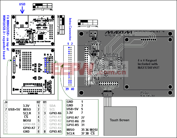 图2. 系统图片,使用一个3M内部连接器来连接MINIQUSB+和MAX1234评估板。