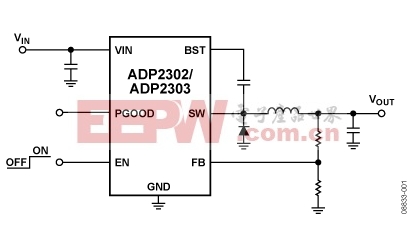
ADP2302/ADP2303典型应用电路图
作者:dolphin
时间:2012-07-31
ADP2302/ADP2303典型应用电路图
ADP2302/ADP2303,pdf datasheet
特性:
Wide input voltage range: 3.0 V to 20 V
Maximum load current: 3 A for ADP2303
±1.5% output accuracy over temperature range
Output voltage down to 0.8 V
700 kHz switching frequency
Current-mode control architecture
Automatic PFM/PWM mode switching
Precision enable pin with hysteresis
Integrated high-side MOSFET
Integrated bootstrap diode
Internal compensation and soft start
Power-good output
Undervoltage lockout (UVLO)
Overcurrent protection (OCP)
Thermal shutdown (TSD)
8-lead SOIC package with exposed paddle
关键词: 电子电路图,ADP2302

加入微信
获取电子行业最新资讯
搜索微信公众号:EEPW
或用微信扫描左侧二维码