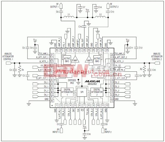
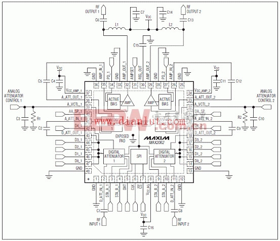
MAX2062应用电路
 Since each of the stages has its own external RF input and RF output, this component can be configured to either optimize noise figure (NF) (amplifier configured first), OIP3 (amplifier last), or a compromise of NF and OIP3. The device’s performance features include 24dB amplifier gain (amplifier only), 7.3dB NF at maximum gain (includes attenuator insertion losses), and a high OIP3 level of +41dBm. Each of these features makes the device an ideal VGA for multipath receiver and transmitter applications.In addition, the device operates from a single +5V supply with full performance or a +3.3V supply for an enhanced power-savings mode with lower performance. The device is available in a compact 48-pin TQFN package (7mm x 7mm) with an exposed pad. Electrical performance is guaranteed over the extended temperature range, from TC = -40°C to +85°C.
Key Features
- Independently Controlled Dual Paths
- 50MHz to 1000MHz RF Frequency Range
- Pin-Compatible Family Includes
- MAX2063 (Digital-Only VGA)
- MAX2064 (Analog-Only VGA)
- 19.4dB (typ) Maximum Gain
- 0.34dB Gain Flatness Over 100MHz Bandwidth
- 64dB Gain Range (33dB Analog Plus 31dB Digital)
- 56dB Path Isolation (at 200MHz)
- Built-In 8-Bit DACs for Analog Attenuation Control
- Supports Four Rapid-Fire Preprogrammed Attenuator States
- Quickly Access Any One of Four Customized Attenuator States
- Ideal for Fast-Attack, High-Level Blocker Protection
- Protects ADC Overdrive Condition
- Excellent Linearity (Configured with Amp Last at 200MHz)
- +41dBm OIP3
- +56dBm OIP2
- +19dBm Output 1dB Compression Point
- 7.3dB Typical Noise Figure (at 200MHz)
- Fast, 25ns Digital Switching
- Very Low Digital VGA Amplitude Overshoot/Undershoot
- Single +5V Supply (or +3.3V Operation)
- Amplifier Power-Down Mode for TDD Applications
MAX2062,pdf: http://www.elecfans.com/soft/39/2010/2010121997860.html
Applications/Uses
Fixed Broadband Wireless Access
GSM/EDGE Base Stations
IF and RF Gain Stages
Military Systems
Temperature-Compensation Circuits
WCDMA, TD-SCDMA, and cdma2000® Base Stations
WiMAX, LTE, and TD-LTE Base Stations and Customer-Premise Equipment
Wireless Local Loop
关键词: 电子电路图,MAX2062

加入微信
获取电子行业最新资讯
搜索微信公众号:EEPW
或用微信扫描左侧二维码