UCC27210参考设计电路|高频高侧/低侧驱动器应用电路
UCC27210特性:最大引导电压120V直流;4A吸收,4A源输出电流;2ns延迟匹配;-40℃至140℃的额定温度范围
UCC27210典型应用范围:半桥和全桥转换器;D类音频放大器;有源箝位正激式转换器;高电压同步降压型转换器
UCC27210参考设计应用电路:
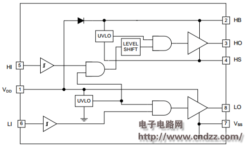
图1UCC27210内部结构图
TheUCC27210 devices represent Texas Instruments’ latest generation of high voltage gate drivers which are designed to drive both the high side and low side of N-channel MOSFETs in a half-/full-bridge or synchronous buck configuration. The floating high-side driver can operate with supply voltages of up to 120 V.
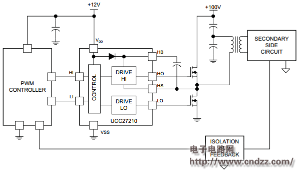
图2UCC27210参考设计图
Theswitching node (HS pin) of the UCC2721x can handle –18 V maximum which allows the high-side channel to be protected from inherent negative voltages caused parasitic inductance and stray capacitance. The UCC27210 (Pseudo-CMOS inputs) and UCC27211 (TTL inputs) have increased hysteresis allowing for interface to analog or digital PWM controllers with enhanced noise immunity.
UCC27210中文数据手册:点击下载
更多原理图及源代码热门应用电路:立刻点击

加入微信
获取电子行业最新资讯
搜索微信公众号:EEPW
或用微信扫描左侧二维码