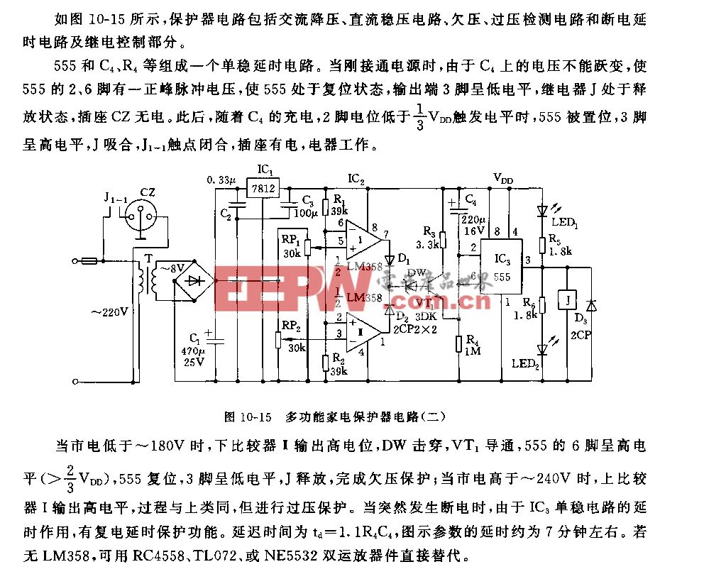
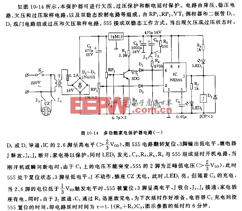
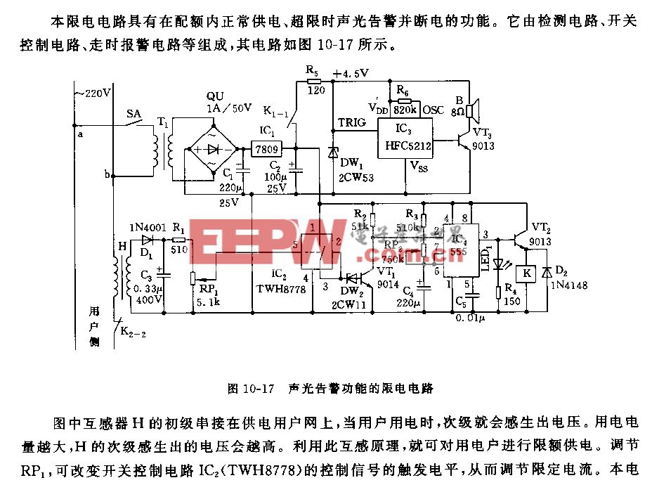
TPS53515参考设计电路|同步降压转换器应用电路
作者:沉默的offer
时间:2018-07-27
TPS53515是一款具有自适应接通时间D-CAP3控制模式的小尺寸、同步降压转换器。此篇主要介绍了TPS53515特性、应用范围、参考设计电路以及电路分析,帮助大家缩短设计时间。
TPS53515特性:12A连续输出电流;输出电压范围:0.6V到5.5V;内置输出放电电路;开漏电源正常输出
TPS53515典型应用范围:服务器和云计算负载点;宽带、网络、光通信基础设施;I/O电源
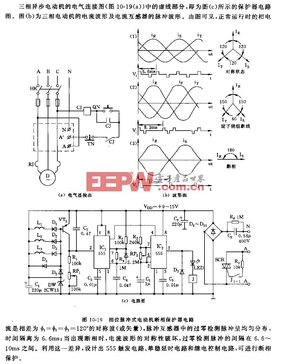
TPS53515参考设计应用电路:
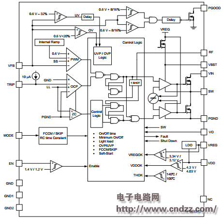
图1TPS53515内部结构图
TheTPS53515 is a high-efficiency, single-channel, synchronous-buck converter. The device suits low-output voltage point-of-load applications with 12-A or lower output current in computing and similar digital consumer applications.
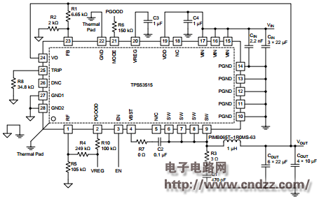
图2TPS53515参考设计图
TheTPS53515 features proprietary D-CAP3 mode control combined with adaptive on-time architecture. This combination builds modern low-duty-ratio and ultra-fast load-step-response DC-DC converters in an ideal fashion. The output voltage ranges from 0.6 V to 5.5 V.
TPS53515中文数据手册:点击下载
更多原理图及源代码热门应用电路:立刻点击

加入微信
获取电子行业最新资讯
搜索微信公众号:EEPW
或用微信扫描左侧二维码