TPS92512参考设计电路|降压电流调节器应用电路
TPS92512特性:集成式200mΩ高侧MOSFET;0V至300mV可调基准电压;开关频率范围为100kHz到2MHz;专有的PWM调光输入
TPS92512典型应用范围:路灯;紧急通道/出口照明;一般工业和商业用照明;灯带
TPS92512参考设计应用电路:
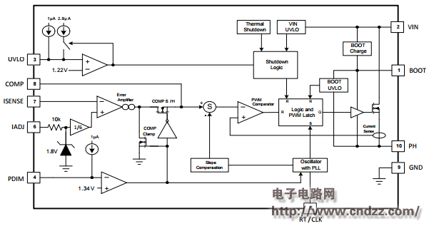
图1TPS92512内部结构图
The TPS92512 is a high voltage, up to 2.5-A, step-down (buck) regulator with an integrated high-side N-channel MOSFET. To improve performance during line and load transients the device implements a constant frequency,peak-current mode control which reduces output capacitance and simplifies external frequency compensation design.
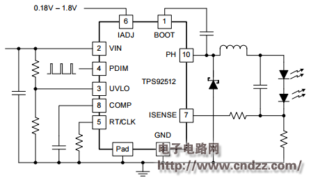
图2TPS92512参考设计图
The TPS92512 contains an internal under-voltage lockout circuit on the VIN pin of the device. However, this internal UVLO is for device protection only and does not contain hysteresis. The UVLO pin of the device should always be used to set the minimum VIN voltage that the circuit operates at. This level should be set using the minimum input voltage expected for the application with a minimum setting of 4.5 V.
TPS92512中文数据手册:点击下载
更多原理图及源代码热门应用电路:立刻点击

加入微信
获取电子行业最新资讯
搜索微信公众号:EEPW
或用微信扫描左侧二维码